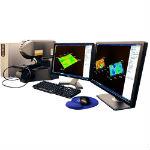
 United States. Michelman said he invested in a new digital imaging technology that allows chemists to view coating and substrate samples with nano-level magnification. The new technology is part of the investment in Michelman's Advanced Materials Collaboration Center that officially opened on October 2 of this year at the company's global headquarters in Cincinnati.
According to the company, this technology that is not widely available in the packaging coatings and specialty chemical industries, allows them to quickly and thoroughly analyze the surface characteristics that are critical for the development of successful coating systems for paper boards, corrugated and flexible cardboard packaging, wood, metal, plastic, concrete and other industrial applications.
The information collected includes high-resolution 3-D and topographic views using rigorous and non-destructive sample preparation measures. Multiple samples can be recorded and compared using various analysis modes. The complete information and large amount of data are used to solve problems, improve or develop coating technologies.
According to Roberto Turnbull, Global Technology Manager, Printing and Packaging, "Our new digital imaging technology is enabling us to help customers solve problem formulations and bring effective new or reformulated products to market faster than ever. Analyses that were previously impossible, or that needed weeks to perform, can now be done in a fraction of the time compared to scanning electron microscopy or other high-resolution techniques."